A DRAM bank is a 2D array of cells. Each address is a <row, column> pair. When a data location needs to be accessed, the relevant row is transferred into a Row Buffer. The data at a specific column of the row is then retrieved. This process is shown below
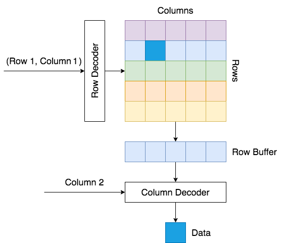
The Row Buffer can only hold one row at a time. The processor interacts only with the data that is present in the Row Buffer. When the required data is present in the row that is already loaded in the Row Buffer, the row is called an Open Row. If the given data is present in a different row than the one in the Row Buffer, the row is called a Closed Row.
Access to data in an Open Row is straightforward. The data is indexed using the column number. Access to data in a Closed Row happens in a sequence of steps. First the existing data in the Row Buffer needs to be written back to main memory. This is called precharging. The precharge command closes the current row in the Row Buffer and prepares the bank for the next access. An activate command is issued on the new row index. This brings a new row into the Row Buffer.
Row Access Command
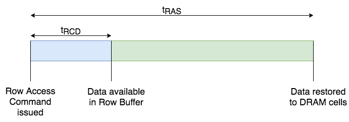
Row Access command moves data from the cells in the DRAM arrays to the Row Buffer. This command is also responsible for restoring the data back into the cells in the DRAM arrays.
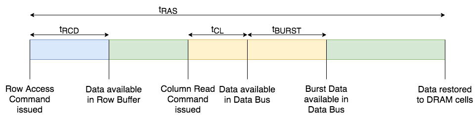
The time it takes for the Row Access command to move data from the DRAM cell arrays to the Row Buffer is known as the Row-Column (Command) Delay,  .
.
After time, the entire row of activated data is held in the Row Buffer, and subsequent column read/write commands can then move data between the Row Buffer and the Memory Controller through the data bus.
A write command will update the data in the Row Buffer. This data is not fully restored back to the cells of the DRAM array. The time it takes for a Row Access command to move the data into the Row Buffer, perform read/write operations and restore the data back into the DRAM cells is known as the Row Access Strobe latency,  .
.
After time the Row Buffer is assumed to have completed data restoration to the DRAM arrays, and the Row Buffer can then be precharged for another Row Access.
Column Read Command
A Column Read command moves data from the Row Buffer of a given bank of DRAM arrays through the data bus back to the Memory Controller.
The Column Access Strobe Latency,  or
or  is the time it takes for the DRAM device to place the requested data onto the data bus after issuance of the Column Read command.

Generally a burst of data (say  cells) is issued instead of just a single column of data. The duration of the data burst on the data bus for a single column-read command is labelled as
  or
or  .
.
Precharge Command
The Precharge command completes the Row Access sequence as it resets the Row Buffer prepares for another Row Access command.
Row Precharge Time,  time after the assertion of the Precharge command, the Row Buffer of the selected bank is properly precharged.
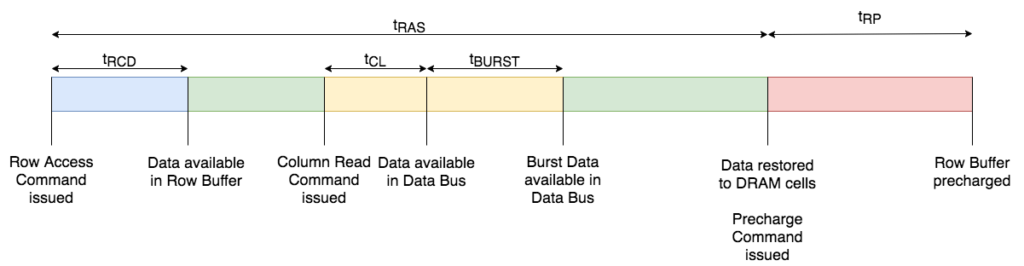
The Row Cycle Time,  is the amount of time that a DRAM device needs to bring data from the DRAM cell arrays into the Row Buffer, perform read/write operations, restore the data back to the DRAM cells, and precharge the Row Buffer for another row access command.


Refresh Command
The electrical charge stored in the storage capacitors will gradually leak out through the access transistors. To ensure data integrity, the Refresh command reads and restores the data in DRAM devices.
DRAM devices use a Refresh Row Address Register to keep track of the address of the last refreshed row. The memory controller sends a single refresh command to the DRAM device, and the DRAM device increments the address in the refresh row address register and goes through a row cycle for all rows with that row address in all of the banks in the DRAM device.
The same row address is sent to all banks to be refreshed concurrently. A single refresh command to all banks takes one Refresh Cycle Time,  .
.
Example
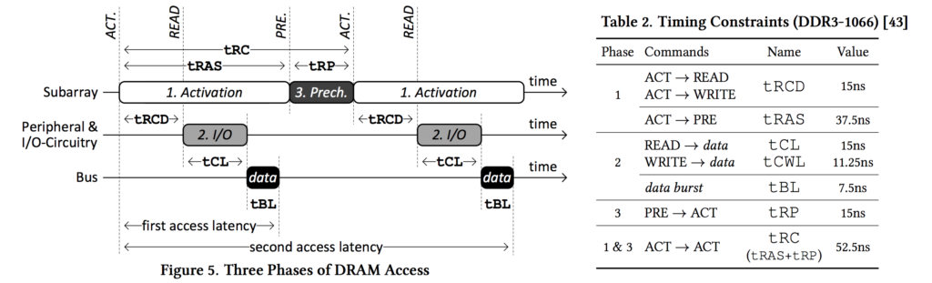
The following figure shows the phases of DRAM access and example timings. This figure also mentions Column Write timing which is similar to Column Read.
Memory Timings
Memory timings describe the performance of SDRAM using four parameters: , , , and in units of clock cycles. They are commonly written as four numbers separated with dashes, e.g.  . When translating memory timings into actual latency, it is important to note that they are in units of bus clock cycles, which for double data rate (DDR) memory is half the speed of the commonly quoted transfer rate.
For example, DDR3- memory has a
  MHz clock frequency, which yields a
  ns clock cycle. With this ns clock,
  gives an absolute latency of
  ns. Faster DDR3-
 (with a
  MHz clock, or
  ns per cycle), may have a larger
  , but that still results in a shorter absolute latency of
  ns.
ns.
Here is a summary of the four parameters
| Name | Symbol | Definition |
|---|---|---|
| CAS Latency | | The number of cycles it takes to read the first bit of memory from a DRAM with the correct row already open. |
| Row Address to Column Address Delay | | The time to read the first bit of memory from a DRAM without an active row is  . . |
| Row Precharge Time | | The time to read the first bit of memory from a DRAM with the wrong row open is  |
| Row Active Time | | The time needed to internally refresh the row, and overlaps with . In SDRAM modules, it is simply  . Otherwise, approximately equal to . Otherwise, approximately equal to  . . |