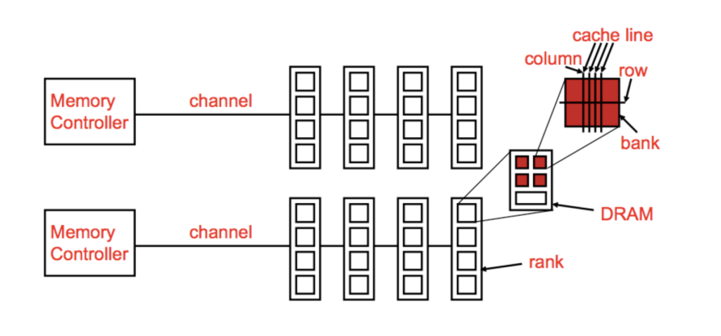
The above figure shows the generalized (5-dimensional) structure of a DRAM. There are  independent memory controllers. Each memory controller is connected to
  DIMMs via a channel. Each DIMM has
  rank. Each rank has DRAM chips. Each chip has (red) banks. Each bank is a -D structure of rows and columns.
Channel
The connection path between the Memory Controller and the DRAM module(s) is called a channel. A logical channel is the source part of the connection from the Memory Controller. A physical channel is the destination part of the connection at the DRAM module(s). For a single Memory Controller, the DRAM module(s) operate in lockstep across all the physical channels. Adding multiple independent Memory Controllers increases bandwidth.
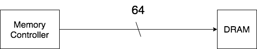
 bits wide, One logical channel bits wide
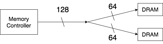 bits wide each, One logical channel
  bits wide
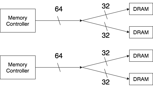
 bits wide each, Two logical channel bits wide each
Memory Module
Memory modules are miniature system boards that hold a number of DRAM chips. These modules are plugged into the motherboard.
In Single In-Line Memory Modules the contacts on either side of the bottom of the module are electrically identical. In Dual In-Line Memory Modules (DIMM) the contacts on either side the module are electrically different.
Rank
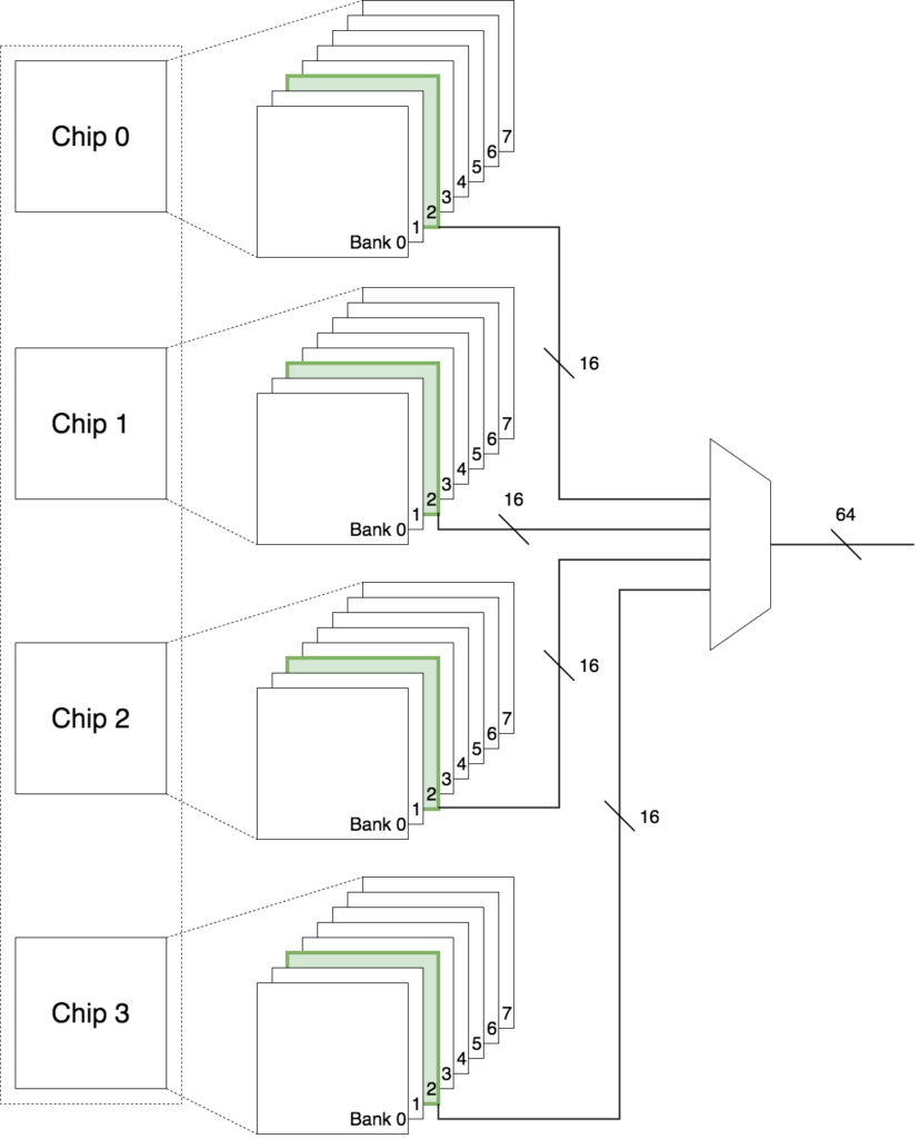
A rank of memory is a subset of DRAM chips in a Memory Module that operate in lockstep in response to a given command. All chips comprising a rank are controlled at the same time. They share the address and command buses but provide different data.
For example, a single-sided DIMM typically comprise of only a single rank of  DRAM chips. In other words, all the DRAM chips on one side of the DIMM constitute a rank. A double-sided DIMM with a total of
  DRAM chips can be divided into two ranks of DRAM chips each. In other words, each side of the DIMM constitutes a rank.
ranks of DRAM chips each. Each side of the DIMM constitutes a rank.Bank
A bank is a set of independent arrays inside a DRAM chip. Each bank of memory is an independent array that can be in different phases of a data access/refresh cycle. These access can be pipelined.
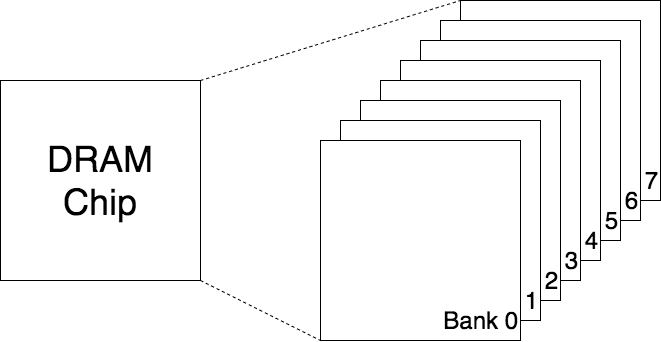 banks.
It is important to note that the same bank location is accessed simultaneously across all the DRAM chips within a rank. For example, consider a rank of DRAM chips. bytes of data needs to be read from a location in Bank . In this case, each DRAM chip will contribute bytes of data from their respective banks. In a way, organizing the DRAM chips into ranks, gives the Memory Controller the illusion that it can interact with a high capacity single DRAM chip.
Row
A row is a group of storage cells that are activated in parallel in response to a row activation command. A row can be visualized as the horizontal segment of a bank. A row activation command will activate the same addressed row (of a bank) in all DRAM chips in a given rank of memory. From the perspective of the memory controller, the size of a row is the size of a row in a given DRAM chip multiplied by the number of DRAM chips in a given rank. Thus, a DRAM row spans across the multiple DRAM chips of a given memory.
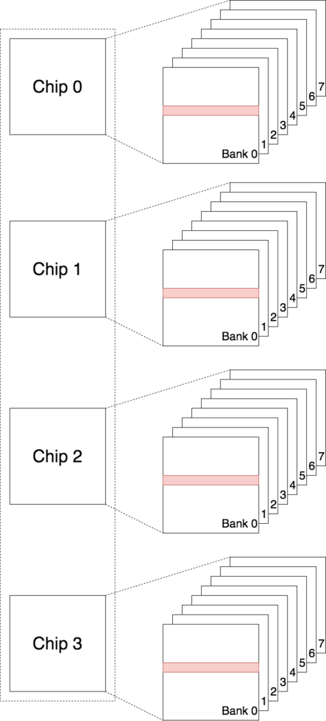
 spanning across DRAM Chips in a rank.
Column
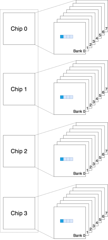
A column of data is the smallest addressable unit of memory. In DDRx SDRAM memory systems, each column access command can fetch multiple columns of data depending on the programmed burst length.
 .
.Beat
A beat is a data transition on the data bus. In SDRAM memory systems, there is one data transition per clock cycle. In DDRx SDRAM memory systems, two data transfers can occur in each clock cycle, so two beats of data are transferred in a single clock cycle.
| Memory System | Clock Cycle | Beats of Data |
| SDRAM | | |
| DDRx SDRAM | | |
Burst
Each column access command can fetch multiple columns of data depending on the programmed burst length. For example, on a DDR2 DRAM device, each memory read command returns a minimum of columns of data.
Example Configurations
Assume that Column holds byte of data.
| # Rows | # Columns | # Banks | Chip Capacity | Chips/Rank | # Ranks | DRAM Capcity |
 |  |  |  |  |  |  |
 |  | | MB | | |  MB MB |
|  | | MB | | | MB |
| | | MB | | | MB |
 | | | MB | | | MB |